About Me
I am an electrical engineer with a PhD from KU Leuven, obtained in 2024 under the supervision of Prof. dr. ir. Ingrid Verbauwhede. My research focused on the design and analysis of hardware implementations of cryptographic primitives, including True Random Number Generators (TRNGs) and Physical Unclonable Functions (PUFs). During my PhD, I successfully taped out three ASICs, further developing my expertise in digital design, which remains my primary area of interest.
Design Experience
Pipelined Architecture for TRNGs
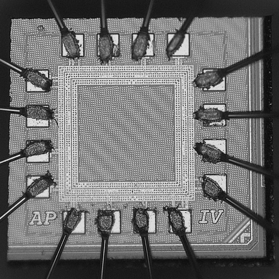
This ASIC features a fully digital TRNG with increased Time-to-Digital Converter (TDC) resolution enabled by a Vernier Delay Line (VDL) technique. It incorporates concurrent jitter accumulation, forming a jitter pipeline to enhance randomness generation efficiency. A stochastic model is available, ensuring compatibility with modern TRNG standards such as NIST SP 800-90B and AIS 20/31.

Energy- and Area-Efficient Entropy Source
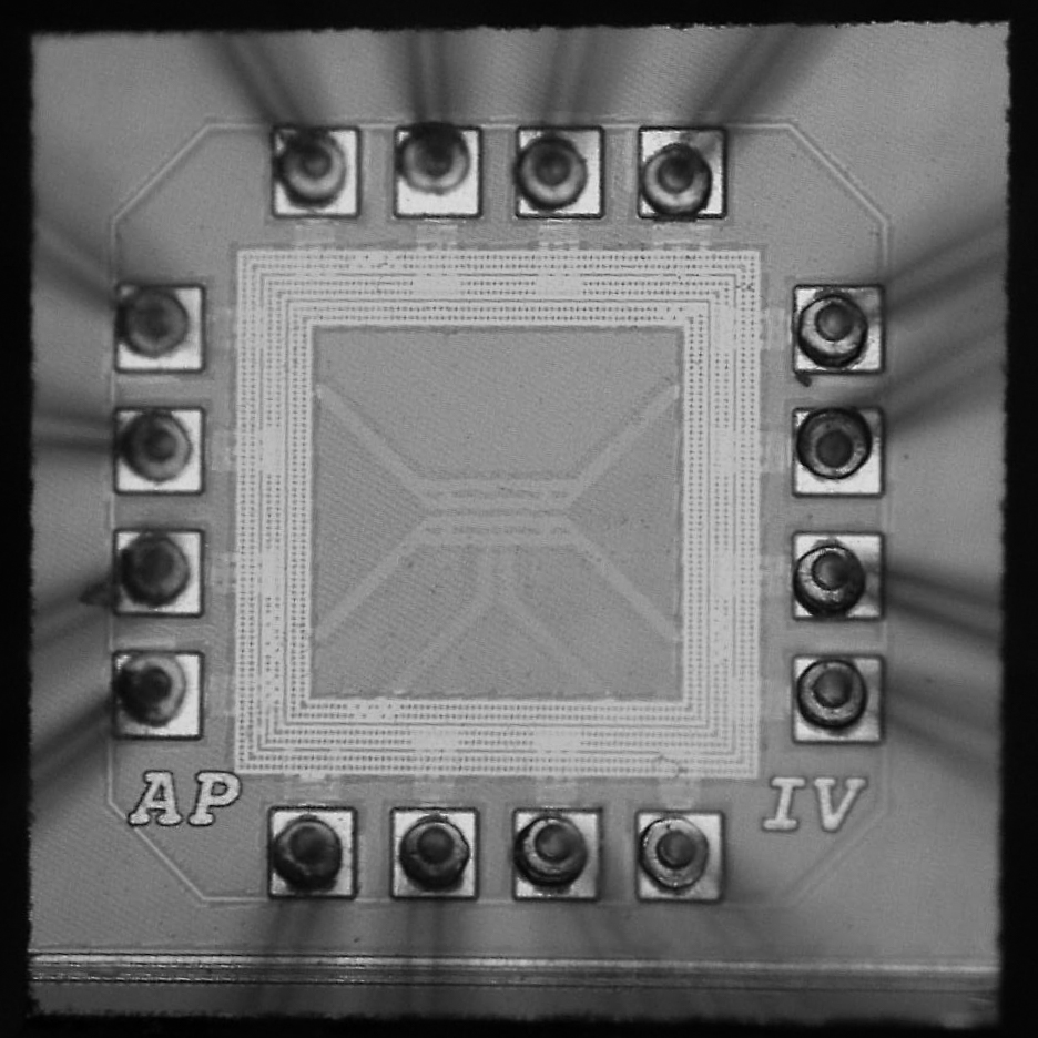
This ASIC features an energy- and area-efficient entropy source for TRNGs, accompanied by a comprehensive stochastic model. It employs a jitter pipelining architecture with enhanced timing resolution to maximize throughput and energy efficiency. The fully digital design ensures seamless portability to other technology nodes, leveraging the benefits of technology scaling. Additionally, the design complies with modern TRNG standards, including NIST SP 800-90B and AIS 20/31.

Characterization of RO Jitter & Multi-Edge Entropy Source
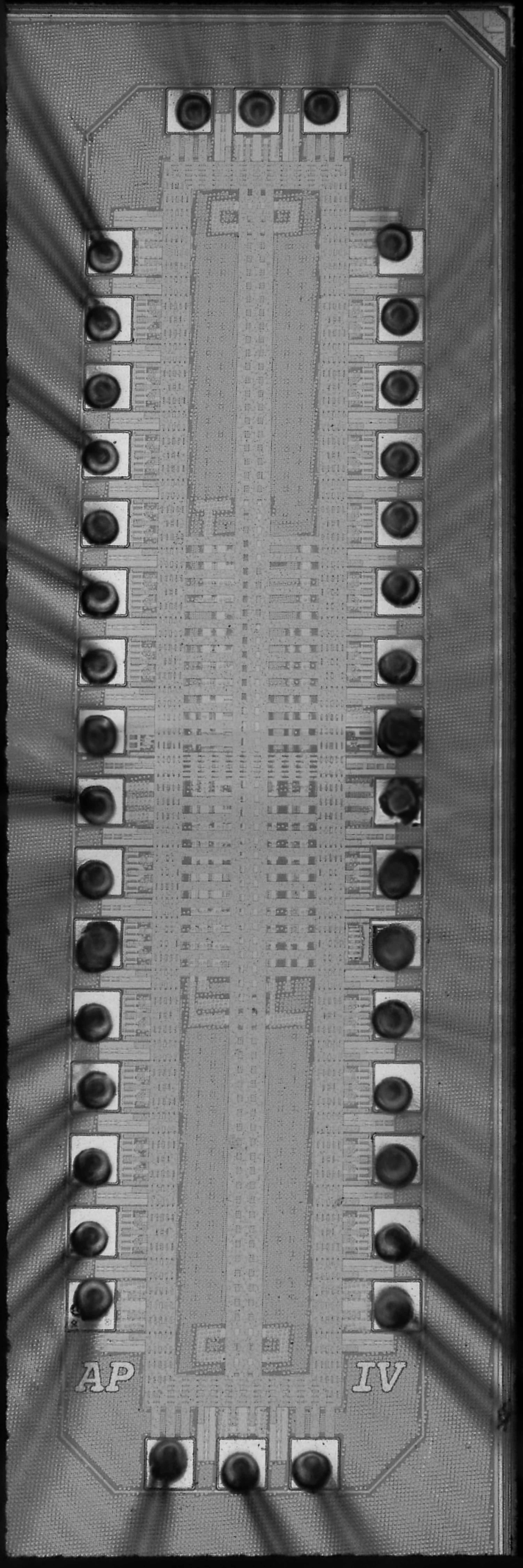
This ASIC features two subcircuits: a jitter characterization module and a multi-edge Ring Oscillator (RO) entropy source. The jitter characterization hardware, utilizing delay chain time-to-digital conversion, enables the analysis of dominant noise types in free-running ROs. A time-domain study analytically links the oscillator excess phase variance to the accumulation time length. The multi-edge RO entropy source concurrently extracts entropy from multiple racing edges, improving throughput and energy efficiency.

Patents
Random Number Generator
This patent introduces a configurable RO architecture that leverages logic gate propagation delay variability to enable a tunable range of oscillation frequencies. The fully digital design is compatible with both FPGAs and ASICs, ensuring versatile deployment. The architecture is suitable for various oscillator-based entropy sources, with a detailed implementation example provided for the Coherent Sampling RO (COSO) entropy source.
